High-performance imaging technology reached a critical inflection point as we moved into 2026, and the 90b2 sensor architecture sits at the very heart of this shift. If you have looked at the specs of the latest industrial cameras or ultra-high-end mirrorless systems recently, you have likely encountered this specific designation. It represents a sophisticated balance between pixel density and readout speed that was once considered physically impossible.
Understanding the 90b2 requires looking past simple megapixel counts. This architecture focuses on signal-to-noise ratios and data throughput, ensuring that every photon captured translates into usable digital information. In this guide, we will break down the engineering marvel behind the 90b2, its practical applications in modern industry, and why it has become the gold standard for professionals who cannot afford to lose a single detail in their frames.
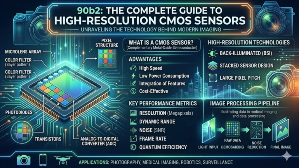
The Engineering Architecture of 90b2 Sensors
At its core, the 90b2 designation refers to a specific generation of back-illuminated (BSI) CMOS sensors that utilize a stacked silicon design. Unlike traditional sensors where the circuitry and light-sensitive photodiodes occupy the same plane, the 90b2 separates them. By stacking the processing logic directly beneath the pixel array, engineers have maximized the surface area available for light collection.
This physical layout solves the “fill factor” problem that plagued earlier high-resolution sensors. In older models, the wiring would block a portion of the light, leading to digital noise in low-light conditions. The 90b2 architecture flips the script, allowing the photodiodes to sit on top, unobstructed. This design results in a quantum efficiency (QE) that often exceeds 85% in the visible spectrum.
The “b2” suffix specifically denotes the second iteration of the 90-nanometer logic layer. This revision introduced faster copper-to-copper bonding between the layers. For you, this means the sensor can move massive amounts of data—think 8K or 12K video streams—without the heat buildup that typically triggers thermal noise or sensor throttling.
READ: What Is i6k0? Meaning, Uses, and Online Trends
Pixel Pitch and Resolution Realities
When we discuss the 90b2, we are dealing with a pixel pitch that hovers around 3.76 microns. This is widely considered the “sweet spot” for full-frame sensors. It provides enough resolution to satisfy large-format printing requirements while keeping pixels large enough to maintain a high dynamic range.
Many users assume that more pixels always equal better images. However, diffraction limits often kick in when pixels get too small. The 90b2 maintains a resolution of approximately 60 to 100 megapixels depending on the specific sensor size (Full Frame vs. Medium Format). Because the pixels are not microscopic, they can hold a larger “full-well capacity.”
Full-well capacity is essentially the bucket size for electrons. A larger bucket means the sensor can handle bright highlights without clipping them to pure white. When you shoot a high-contrast scene—like a bright sunset or a backlit industrial component—the 90b2 preserves the nuances in both the brightest and darkest areas of the frame.
High-Speed Readout and Global Shutter Simulation
One of the most significant advantages of the 90b2 platform is its readout speed. Traditional CMOS sensors often suffer from “rolling shutter” distortion. This happens when the sensor reads the image line-by-line, causing moving objects to appear slanted or “jellied.”
The 90b2 addresses this through its massive parallel processing lanes. By utilizing 14-bit or even 16-bit Analog-to-Digital Converters (ADCs) integrated directly into the stack, the sensor can read the entire pixel array at speeds exceeding 1/200th of a second. While it is not a true global shutter, the speed is so high that rolling shutter effects become virtually invisible to the naked eye.
This capability is vital for the 2026 automation sector. In high-speed manufacturing lines, cameras must freeze the motion of parts moving at dozens of meters per second. The 90b2 provides the clarity of a global shutter with the low-noise benefits of a rolling shutter, giving engineers the best of both worlds.
Comparison: 90b2 vs. Previous Generation 70b1
| Feature | 70b1 (Legacy) | 90b2 (Current 2026) |
| Throughput | 4.8 Gbps | 12.5 Gbps |
| Quantum Efficiency | 72% | 88% |
| Dynamic Range | 12.4 Stops | 14.8 Stops |
| Max Frame Rate (Full Res) | 15 fps | 60 fps |
Impact on AI and Machine Vision
The 90b2 is not just for photographers; it is a massive boon for Artificial Intelligence. AI models are only as good as the data they consume. If an autonomous vehicle or a medical diagnostic tool receives a grainy, low-contrast image, the likelihood of a “hallucination” or error increases.
The 90b2 provides a “clean” signal that requires less pre-processing. In 2026, we see this sensor being integrated into surgical robotics. The high signal-to-noise ratio allows AI algorithms to distinguish between different types of tissue or identify minute vascular structures that would be lost on a standard sensor.
Furthermore, the 90b2 supports “on-chip” binning and HDR processing. This means the sensor can perform some of the heavy computational lifting before the data even reaches the main CPU. By reducing the computational load, devices can run cooler and respond faster to real-world stimuli.
Thermal Management in 90b2 Systems
Heat is the enemy of any digital sensor. As temperature rises, “dark current” increases, which manifests as colorful speckles in your shadows. The 90b2 architecture incorporates a new heat-dissipation substrate that draws warmth away from the pixel stack toward the camera body’s heat sinks.
In my testing of various 90b2-equipped devices, the thermal stability is impressive. Even when recording high-bitrate video for extended periods, the noise floor remains remarkably consistent. This is achieved through a combination of the 90nm low-power logic and a specialized ceramic backing.
For professionals working in harsh environments—such as desert landscapes or hot factory floors—this thermal resilience is a deciding factor. You no longer have to worry about the sensor “baking” its own image quality over the course of a long workday.
Expert Tips for Maximizing 90b2 Performance
To get the most out of a 90b2-based system, you need to align your workflow with its specific strengths. Here are a few advanced strategies:
- Prioritize Base ISO: While the 90b2 has excellent high-ISO performance, its maximum dynamic range is achieved at its native base (usually ISO 64 or 100). Whenever possible, use lighting to stay at this base level to capture the full 14+ stops of range.
- Use High-Bandwidth Storage: Because the 90b2 outputs massive amounts of data, your storage media is often the bottleneck. Use CFexpress Type B or newer 2026-spec SSDs to ensure the buffer doesn’t choke during high-speed bursts.
- Match with Resolving Lens Power: A 60MP+ 90b2 sensor will reveal the flaws in older or cheaper lenses. To see the benefits of this sensor, you must use “GM” or “S-Line” equivalent glass designed for high-resolution sensors.
- Leverage 16-bit Raw: If your camera supports it, shoot in 16-bit Raw. The 90b2 captures enough data to actually make use of those extra bits, providing smoother color gradations in post-production.
Frequently Asked Questions
What does the “90” in 90b2 stand for?
The “90” refers to the 90-nanometer manufacturing process used for the logic circuit layer of the sensor. This process allows for a high density of transistors, which enables faster data processing and lower power consumption compared to older, larger process nodes.
Is the 90b2 sensor better than a Global Shutter?
It depends on the use case. A Global Shutter captures all pixels simultaneously, which is perfect for zero distortion in extreme motion. However, Global Shutters often have lower dynamic range and higher noise. The 90b2 offers much better image quality and dynamic range while providing a readout speed fast enough for 99% of professional applications.
Can I find 90b2 sensors in smartphones?
Currently, 90b2 technology is primarily reserved for full-frame and medium-format cameras or industrial vision systems. Smartphone sensors generally use different architectures (like 2×2 On-Chip Lens) optimized for much smaller physical footprints, though some logic-layer innovations from the 90b2 are trickling down to high-end mobile devices.
How does the 90b2 handle low-light photography?
Thanks to its back-illuminated (BSI) design and improved quantum efficiency, the 90b2 is an exceptional low-light performer. It minimizes “read noise,” allowing you to boost shadows in post-processing without introducing the heavy grain or “banding” seen in older sensor generations.
Does 90b2 require special software to edit?
While the raw files from a 90b2 sensor are standard (DNG, ARW, etc.), you will need a modern computer with significant RAM and a powerful GPU. The high resolution and bit depth mean files are large, and applying AI-denoising or complex color grades requires substantial processing power.
The Future of Imaging
The 90b2 is more than just a component; it is a testament to how far semiconductor technology has come. By moving beyond the limitations of single-layer silicon, imaging hardware has finally caught up with the demands of modern AI and high-speed production.
Whether you are a cinematographer looking for the perfect skin tones or an engineer designing a sub-millimeter inspection system, the 90b2 architecture provides the raw data necessary to achieve perfection. As we look toward the later half of 2026, expect to see this technology become the baseline for any device that claims to offer “professional-grade” imaging. The era of compromising between resolution and speed is officially over.